Georgia Tech Researchers Pioneer Electron Beam Technique for Nanoscale Copper Fabrication
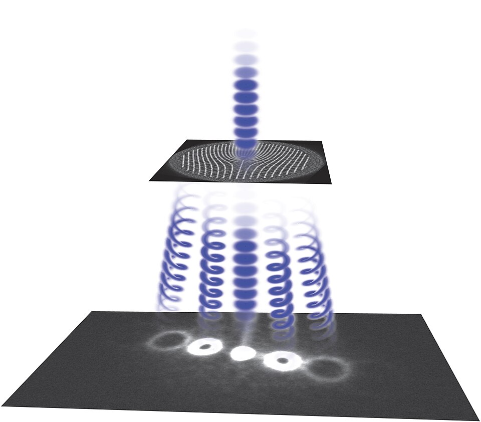
In a groundbreaking study published on July 25, 2025, in the journal Advanced Functional Materials, researchers from the Georgia Institute of Technology have introduced a novel electron beam method that enables the precise carving and building of copper structures at the nanoscale. This innovative technique, developed by Professor Andrei Fedorov and his team at the George W. Woodruff School of Mechanical Engineering, utilizes focused electron beams in a liquid environment to either remove or deposit copper, depending on the chemical composition of the surrounding solution.
The significance of this research lies in its dual capability to etch and deposit materials within the same setup, a departure from conventional methods that typically specialize in one function. The team found that by adjusting the ammonia concentration in the water-ammonia solution, they could control the electron beam's effect on copper: low ammonia concentrations favored etching, while higher concentrations promoted copper deposition. This dynamic switching ability allows for real-time 3D sculpting at the atomic level, a feat that could revolutionize fields such as nanotechnology and materials science.
According to Auwais Ahmed, the lead author of the study and a Ph.D. student at Georgia Tech, “By carefully adjusting the ammonia concentration and the electron beam exposure, we can fine-tune the shape and structure of the copper surface with nanometer precision.” This precision is critical for developing ultra-sensitive scientific tools and nanoscale devices, including microscopic probes, sensors, and advanced wiring for next-generation computer chips.
The implications of this research extend beyond copper. The chemically tunable nature of the method suggests potential applications in other materials as well, paving the way for a flexible tool in nanoscale manufacturing. "This gives us a flexible new tool for nanoscale manufacturing," Ahmed added. "By controlling the local chemistry, we can essentially 3D print and subtract at the same time—opening up new possibilities for design and fabrication in nanotechnology."
The study's findings also highlight the importance of ammonia in the etching and deposition processes. As stated by Fedorov, "Ammonia does several important things. It helps carry copper atoms in solution, neutralizes unwanted reactions, and makes the environment more favorable for building instead of etching." This multifaceted role of ammonia underscores the intricate interplay between chemistry and electron beam technology in achieving nanoscale fabrication.
In addition to its immediate applications, this research could have far-reaching impacts on various industries, including electronics, healthcare, and materials engineering. As the demand for miniaturized devices continues to grow, the ability to manipulate materials with such precision will be crucial.
In conclusion, the electron beam method pioneered by Georgia Tech researchers represents a significant advancement in nanofabrication techniques. With further research and development, this technology could lead to the creation of unprecedented nanoscale devices and structures, offering exciting possibilities for future technological innovations.
Advertisement
Tags
Advertisement